
Services

Semiconductor CNC Machining

We provide precision CNC machining services for the semiconductor industry. Leveraging our expertise in precision manufacturing and complex assembly, we help semiconductor equipment manufacturers achieve optimal accuracy and efficiency in their production processes.

Semiconductor CNC Machining Supplier

In the semiconductor industry, where the pursuit of extreme precision is the gold standard, we stand as a leading custom manufacturer, specializing in high-quality, ultra-precision CNC semiconductor machining solutions for equipment. Fully attuned to the industry’s rigorous demands—including zero-contamination requirements, micron-level tolerances, and superior surface finishes—we utilize state-of-the-art 5-axis CNC machining centers and automated inspection systems to produce custom components for a wide range of semiconductor industry. Our expertise extends to the precision machining of specialized, semiconductor-grade materials. With meticulous control over every stage—from ultrasonic cleaning and cleanroom packaging to comprehensive quality traceability—we empower our clients to significantly enhance equipment stability and process yields, serving as your trusted, core technical partner within the semiconductor supply chain.

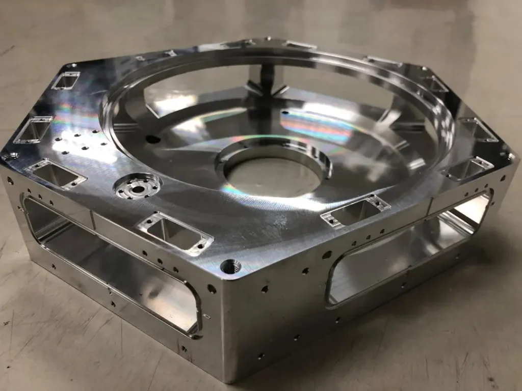
cnc milled aluminum semiconductor chamber
Semiconductor mold pads

Semiconductor CNC Machining for Complex Components

As semiconductor equipment grows more complex, we leverage advanced multi-axis CNC machines to manufacture intricate, high-precision components. Utilizing 5-axis CNC semiconductor machining, optimized toolpaths, and custom fixturing, we easily handle complex geometries—such as multi-cavity structures, thin-walled parts, deep blind holes, and precision flow channels—while eliminating deformation and chatter to maintain stable micron-level tolerances (±0.005 mm). Combined with our deep expertise in semiconductor-grade alloys, engineering plastics, and ceramics, as well as strict cleanroom standards, we deliver high-reliability components with exceptional structural integrity, superior hermetic sealing, and outstanding corrosion resistance to maximize equipment uptime.

Cleanroom Machining Services for Semiconductor Industry

To meet the semiconductor industry’s strict demands for zero-particle residue and high-vacuum purity, we provide specialized cleanroom machining services for the semiconductor industry, establishing a fully integrated clean-manufacturing workflow from controlled processing to ultra-clean delivery. Within controlled environments, we utilize sulfur-free cutting fluids and dedicated toolings to minimize metallic ion and grease cross-contamination. Post-machining, parts undergo multi-stage ultrasonic pure-water cleaning and degreasing bake-out to strictly control material outgassing rates. Every component is verified via particle inspection in our ISO-certified cleanroom and sealed in double-layer anti-static vacuum packaging, ensuring parts are semiconductor-assembly ready straight out of the box.

Cleanroom
Semiconductor CNC Machined Parts 2247

Thermal Management Solutions for Semiconductor CNC Machining

Efficient heat dissipation is critical for semiconductor equipment. We specialize in providing highly reliable thermal management solutions for the semiconductor industry. Leveraging our mission-critical CNC machining capabilities tailored for this sector, we can precisely manufacture complex internal micro-channels and heat-dissipation structures, effectively reducing fluid resistance and eliminating localized "hot spots." Furthermore, by applying ultra-precision mirror-finish machining to thermal interface surfaces—ensuring exceptional flatness and minimal surface roughness—we significantly lower interfacial contact thermal resistance. This effectively mitigates thermal-stress-induced deformation in high-temperature environments, ensuring the efficient and stable operation of thermal control systems in semiconductor equipment.

Semiconductor CNC Machining Capabilities

Our precision CNC machining solutions for the semiconductor sector are designed to enhance the performance and reliability of semiconductor systems. With a focus on precision and efficiency, we manufacture components that ensure your semiconductor equipment consistently operates at peak performance. 

cnc machining service 02

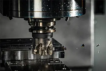
CNC Machining

cnc milling service 02

CNC Milling

cnc turning service02

CNC Turning

CNC milling service 350 1

Mill-Turn Machining

CNC 5 AXIS machining

5 Axis CNC Machining

CNC Surface Grinding scaled

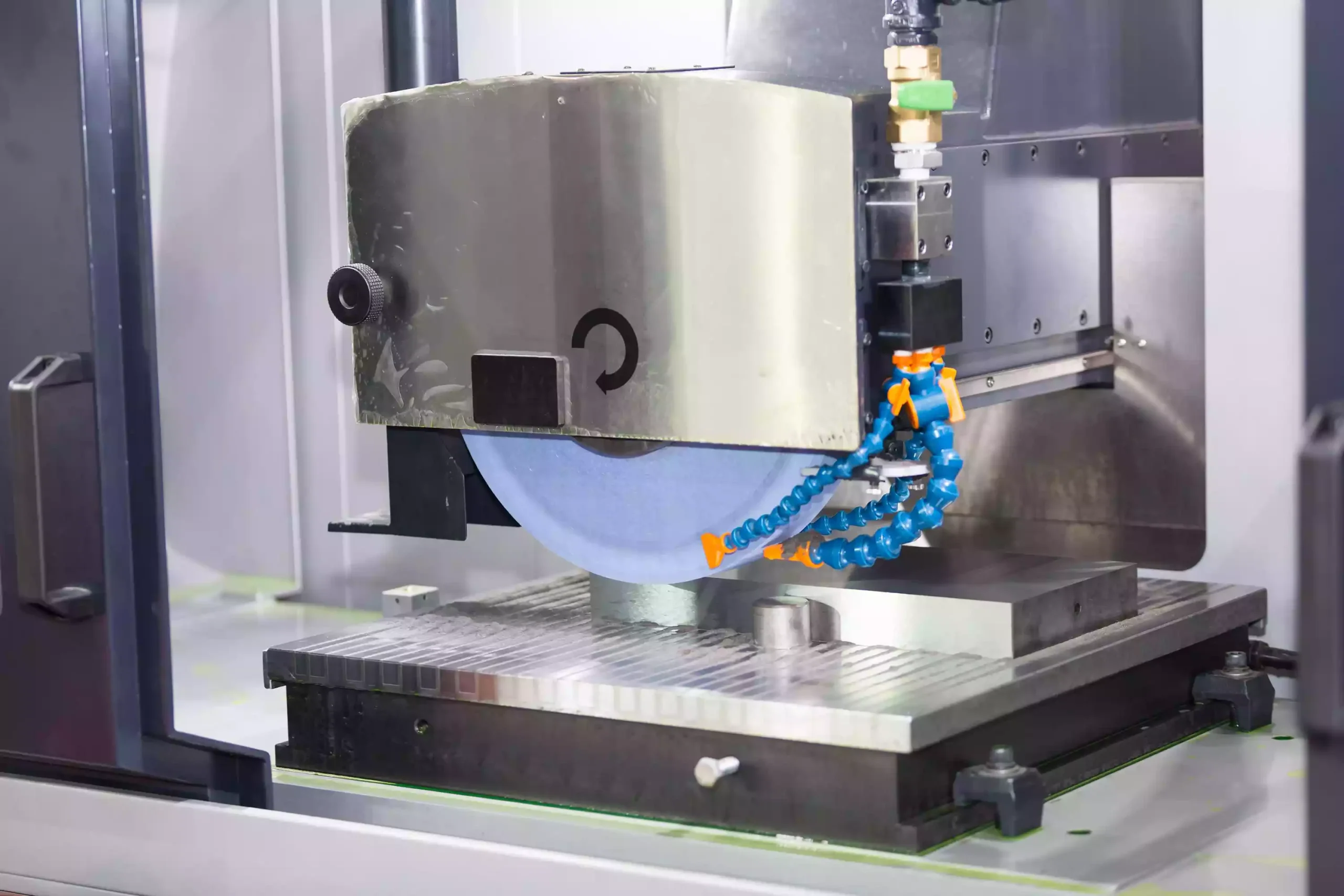
Precision Grinding

MachiningEngenering

Engineering Communication & DFM Support

To help clients shorten equipment R&D cycles and optimize production costs, we offer end-to-end engineering communication & DFM support for CNC semiconductor machining. Our experienced engineering team gets involved early during the NPI (New Product Introduction) phase to conduct thorough Design for Manufacturability (DFM) analyses. We evaluate tolerance stack-ups, tool clearance, hard-to-machine features, and machinability to propose practical design refinements. Without compromising component performance or compliance, our insights help simplify machining operations, improve yields, and drive cost-down solutions. Backed by fluent English technical communication and swift CAD/drawing turnarounds, we bridge time zones seamlessly to accelerate your transition from prototype to full-scale production.

Your Trusted Semiconductor CNC Machining Partner

Xtmade is a custom precision manufacturer based in Shenzhen, China, operating a 120,000-square-foot facility. We provide semiconductor CNC machining services tailored for manufacturers of semiconductor equipment, precision components, and automation systems. Our company is equipped with advanced, high-precision machinery and staffed by a professional team. With years of industry experience and deep technical expertise, our team offers a diverse range of services to meet our clients' needs. From initial blueprints to final product inspection, we provide a one-stop CNC machining semiconductor solution, helping clients transform their existing designs into precision-machined parts that meet all project specifications.

CNC Machining shop 1
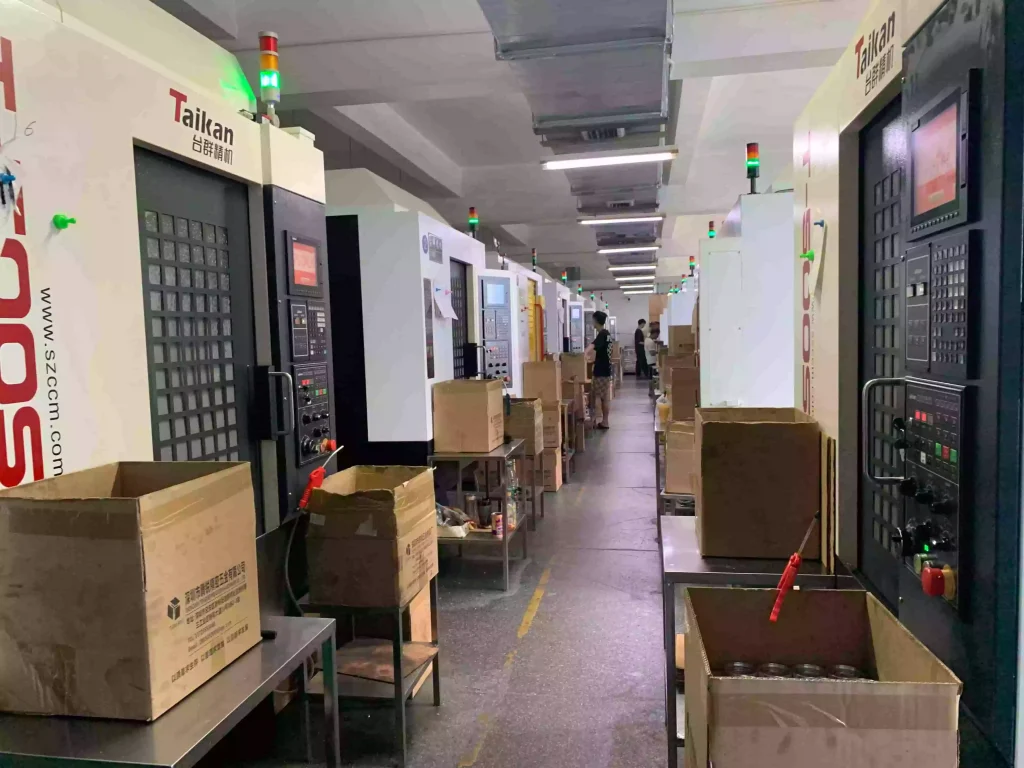
CNC machining production workshop

Semiconductor CNC Machining Shop

To ensure high-volume, reliable production of critical componentry, we have established robust semiconductor CNC machining workshop engineered specifically for high-spec manufacturing. Our facility houses an advanced fleet of German and Japanese 5-axis machining centers, multi-tasking mill-turn machines, and high-speed graphite/ceramic mills, integrated with in-situ Renishaw probing systems and climate-controlled workshops to achieve tight process control across production runs. Complementing our machining hardware, our metrology lab features high-precision CMMs, white-light interferometers, and material spectrometers for end-to-end quality traceability. Supported by flexible manufacturing systems and responsive engineering support, we seamlessly bridge the gap from rapid prototyping to scalable mass production for global semiconductor OEMs.

Quality Assurance

We have established a rigorous quality control system that adheres to semiconductor industry standards, ensuring that every component—from raw materials to the final finished product—meets the highest requirements for precision and purity.

  • First Article Inspection (FAI):Comprehensive dimensional verification against customer drawings before mass production release.
  • In-Process Quality Control (IPQC):Continuous sampling and in-situ probing to monitor dimensional drift and process stability.
  • Outgoing Quality Control (OQC):Final 100% inspection covering critical tolerances, surface integrity, and cleanliness.
  • ISO 9001:2015Certified Quality Management System
  • ISO 14001Environmental Management System
  • RoHS & REACHMaterial Compliance Standards
  • Full compliance with global semiconductor supply chain standards
  • Full Dimensional Inspection Report (CMM Data)
  • Material Test Report (MTR / Mill Certificates)
  • Surface Roughness & Contour Test Report
  • Process Capability (CPK / PPK) Analysis Report
  • Helium Leak Detection & Pressure Test Report (Upon Request)
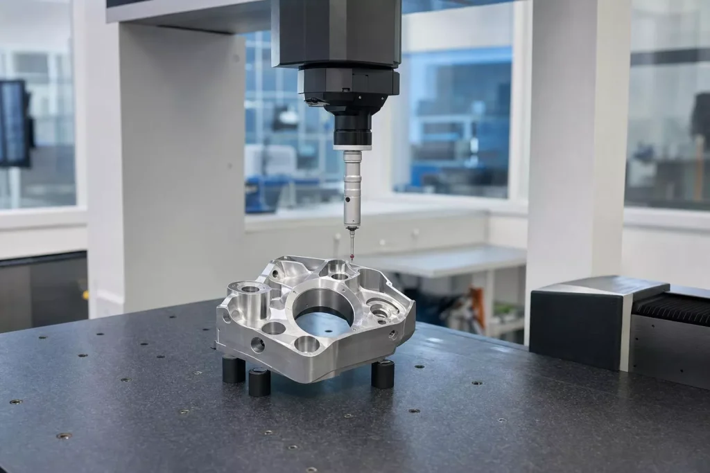
  • High-Precision Coordinate Measuring Machines (CMM):Sub-micron accuracy for geometric and positional tolerance verification.
  • White-Light Interferometer & Profilometer:Ultra-precise micro-surface topography and roughness (Ra) measurement.
  • Video Measurement Systems (VMS):Non-contact optical inspection for micro-features and flexible materials.
  • Optical Emission Spectrometers:Instant raw material chemical composition verification.
  • Helium Mass Spectrometer Leak Detectors:High-sensitivity leak testing for vacuum components.
  •  
quality

Materials for CNC Semiconductor Machining

Material performance directly dictates component corrosion resistance, plasma endurance, and ultra-high purity. To ensure top-tier reliability, we maintain a rigorous selection and processing protocol for materials for CNC semiconductor machining. We possess a deep mastery of the physical and chemical characteristics of semiconductor-grade materials—including resistance to aggressive chemicals, thermal stability and dielectric properties. By tailoring cutting tool geometries and machining parameters to the specific thermal expansion, stress release, and wear behaviors of each substrate, we safeguard material integrity throughout the machining process, delivering good performance for critical semiconductor applications.

Metal

Aluminum gear

Aluminum

Steel gear

Stainless Steel

Titanium gear

Titanium

Kovar gear

Kovar

inconel gear

Inconel

Hastelloy gear

Hastelloy

Plastic

peek

PEEK

ptfe

PTFE

pom

POM

abs

ABS

pet

Polyethylene (PE)

pc

PC

Finish for CNC Semiconductor Machining

In extreme semiconductor environments, surface performance directly dictates equipment longevity and wafer yield. We offer specialized finish options for CNC semiconductor machining tailored to strict semiconductor standards. Through targeted surface modification and ultra-fine refinement, we enhance corrosion and plasma resistance while eliminating micro-flaws. This minimizes outgassing rates in ultra-high vacuum (UHV) environments and prevents particle generation, ensuring long-term surface stability under demanding operational conditions.

anodizing surface treatment services

Anodizing

Electroplating Surface Treatment Services

Electropolishing

Powder Coating

Powder Coating

pvd

PVD

Laser Engraving

Laser Carving

deburring

Deburring

Nickel Plating

Nickel Plating

polishing

Polishing

passivation

Passivation

Semiconductor CNC Machining Components We Manufacture

We provide customized CNC machining services for the semiconductor industry, with the capability to manufacture a wide range of components. Listed below are some examples of the parts we produce.

Precision Structural Components

Precision Structural Components

Vacuum System Components 1

Vacuum System Components

semiconductor Thermal Management cnc Components

Thermal Management Components

Wafer Handling Automation Components

Wafer Handling & Automation Components

Metrology Inspection Components

Metrology & Inspection Components

Custom Fixtures Tooling

Custom Fixtures & Tooling

Electric chips removed from Circuit board

Value-Added Services for Semiconductor CNC Machining

Xtmade provides packaging, identification, and shipping support for custom CNC machined semiconductor equipment components. Packaging and handling methods are selected according to component geometry, surface finish, cleanliness requirements, and customer specifications.

Cleaning and protective packaging can be arranged according to material compatibility, surface requirements, and project specifications. Options may include individual component protection, separated packaging, and additional protection against contamination, scratches, and handling damage.

Part identification and batch information can be incorporated into the manufacturing workflow according to customer requirements. Where supported by the project, identification may include part numbers, batch IDs, or QR codes to facilitate receiving inspection, inventory management, and production traceability.

Custom packaging solutions can be selected for components with precision features, finished surfaces, or sensitive geometries. Protective inserts, individual wrapping, and suitable shipping containers help reduce the risk of impact, abrasion, and handling damage during domestic or international transportation.

Industries & Applications

semiconductor equipment oem

Semiconductor Equipment OEMs

tool OEMs, gas integrators, vacuum suppliers, and automation companies.
front end wafer fab

Front-End Wafer Fabrication

Engineered for CVD, ALD, PVD, Etch, Ion Implantation, CMP, and Photolithography tools, delivering UHP chamber hardware and vacuum components.
semiconductor packaging equipment

Semiconductor Packaging

Ultra-clean structural hardware for wire bonding, flip-chip, wafer-level packaging (FOWLP), and 3D IC tools.
display manufacturing

Metrology, Inspection & Displays Equipment

Sub-micron optical mounts and structural frames for CD-SEM, optical inspection, and OLED/microLED equipment.
solar photovoltaic

Photovoltaics & Solar

Custom components for PECVD tools, screen printers, and automated wafer handling systems.
compound semiconductor

Compound Semiconductor Manufacturing

Precision components for SiC, GaN, GaAs, and InP epitaxy, including high-temp MOCVD reactor hardware and MBE chamber parts.

How to Obtain CNC-Machined Components for the Semiconductor Industry?

Upload your files to receive an instant quote (please attach 2D CAD drawings and 3D CAD models in formats such as STEP, IGES, DWG, PDF, STL, or ZIP).

FAQ

For NPI (New Product Introduction) and quick-turn prototype orders, we offer accelerated fabrication with lead times as fast as 5 to 7 business days. For standard production runs, typical lead time is 3 to 4 weeks, depending on material availability, geometric complexity, and specialized surface treatment requirements.

Depending on component geometry, material, and inspection requirements, we target linear machining tolerances down to ±0.005 mm (±5 μm) and hole location accuracy within ±0.002 mm. For critical features such as sealing faces and flatness requirements, achievable tolerances are evaluated based on the drawing specifications and manufacturing feasibility.

We enforce strict corporate IP protection protocols. Prior to receiving any CAD files or technical drawings, we execute standard Non-Disclosure Agreements (NDAs). All customer design data is stored on secure, encrypted servers with restricted internal access on a need-to-know basis. Furthermore, we mandate strict confidentiality agreements with all internal engineering and operational personnel.

No, we do not require an MOQ. We fully support semiconductor equipment R&D with 1-off prototype manufacturing, while maintaining scalable production capacity to seamlessly transition into high-volume series manufacturing.

We provide comprehensive global supply chain logistics, supporting EXW, FOB, DAP, and DDP (Delivered Duty Paid) terms. Partnering with top-tier international couriers and freight forwarders, we handle export compliance, customs clearance, and insured door-to-door delivery with customized anti-vibration packaging.

We operate a 24-hour rapid response system. If any component fails incoming quality inspection, our quality team initiates an immediate Root Cause Analysis (RCA). Non-conforming parts prioritized for fast-track remanufacturing are re-machined and shipped via express air freight at zero additional cost to the client.

Scroll to Top